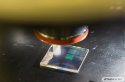
AR technologies have been developing very rapidly in recent years. Developers from different countries create concepts and working prototypes of smart glasses, smart windows, and smart windscreens that can provide users with additional information of what’s happening around them. Hence, the demand for materials to support such solutions is actively growing. They have to be transparent so that users can see through them. At the same time, they also meant to emit light so their surface displays the necessary information.
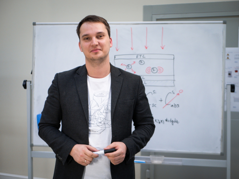
“Creating optoelectronic devices that would fulfil their main functions while staying translucid, flexible, and implementable into glass is a highly promising area,” explains Sergey Makarov, lead researcher at ITMO’s Faculty of Physics and Engineering. “This would allow us to design attractive and functional devices.”
Halide perovskites are one of the promising materials for these purposes. These semiconductor materials are relatively cheap to produce but at the same time they demonstrate high efficiency in solar energy and LED production.
“Perovskite-based solar cells demonstrate over 25% efficiency,” says Sergey Makarov. “While the red and green perovskite LEDs have an external quantum efficiency of over 20%. Moreover, there is an extremely interesting class of devices that operate both as solar cells and LEDs. Such devices are called bifunctional perovskite-based devices.”
Where normal optics fail
It is a highly non-trivial task to create the thinnest films that could be applied to glass and be able to function as AR screens or LEDs. Indeed, it is hard to control the light in such films due to their extremely small thickness.
“When we are talking about active layers thinner than the wavelength at which they operate, and thus several difficulties arise here,” continues Sergey Makarov. “Geometrical optics is no longer applicable here. We need to use nanooptics that allows to optimizing the structure smaller than the wavelength, taking into consideration its complex resonance response.”
As a material for the new coatings, ITMO University researchers with their collaborators from the St. Petersburg National Research Academic University of the Russian Academy of Sciences chose standard perovskite films, which are already used in LED production. The advantage of these films is the presence of their band gap in the visible spectrum that allows transmitting around half of the colors visible to the human eye.
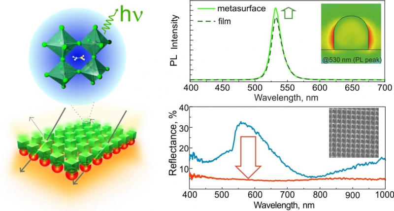
“Initially, these films have a reflection coefficient of about 30%, which means that we lose a third of energy on reflection,” expounds Sergey Makarov. “We aimed at minimizing this reflection loss, so that the surface reflects less and transmits more. This means that users won’t notice they’re looking through a functional layer but it would still keep its useful properties.”
The battle for percent
In order to reduce the reflection coefficient, the researchers had to modify the films and turn them into a metasurface. For this purpose, they removed a part of the perovskite layer and etched a certain strictly periodic pattern of grooves on it. In this form, the surface interacts with light differently.
“Such metasurfaces are well-studied and are produced using other materials such as silicon,” explains Sergey Makarov. “When subjected to a plane wave, each metaatom of this metasurface scatters radiation only forward while backward reflection tends to zero. The effect is known but it’ is a tricky task to implement it in materials with high luminescence (light radiating efficiency).”
The problem is that this pattern has to be applied with nanometer precision. This is usually done with ion nanolithography by bombarding a surface with gallium ions.

“When our colleagues applied these methods to create nanostructures, they noticed that the exposed areas of metasurfaces became dark and burnt out,” explains Tatiana Liashenko, a PhD student at the Faculty of Physics and Engineering. “Even though a lot of the material was left, it did not luminesce under ultraviolet excitation. Unfortunately, this drawback limits the application of such metasurfaces. To solve this problem, we applied the treatment of the perovskite surface by the alcohol salt solution vapour which allowed us to quickly restore the material’s properties.”
Paving the way to a prototype
As a result, the researchers were able to increase the luminescence simultaneously with reducing the reflection coefficient from the sample.

“We divided a thin perovskite film into lots of separated periodically located nanoparticles,” says Kseniia Baryshnikova, the first author of the paper. “Every particle is a rectangular block with a curved “cap”. Each of them interacts with the light in the same way as an antenna interacts with the radio signal, by capturing and redirecting it. The uniqueness of perovskite nanoparticles lies in the fact that under certain geometric parameters (which we were looking for in this paper) they can interact with light similarly in a broad range of the solar spectrum. Thus, most of the energy follows the direction of light. The rest of it is absorbed by the perovskite and transformed into photoluminescence. As a result, we get an active and highly transparent metasurface.”
At the next stage, the researchers will proceed from fundamental research to creating prototypes by implementing the new surfaces into optoelectronic devices.
Reference: Kseniia Baryshnikova, Dmitry Gets, Tatiana Liashenko, Anatoly Pushkarev, Ivan Mukhin, Yuri Kivshar, Sergey Makarov. Broadband Antireflection with Halide Perovskite Metasurfaces, Laser & Photonics Reviews, 2020/10.1002/lpor.202000338


