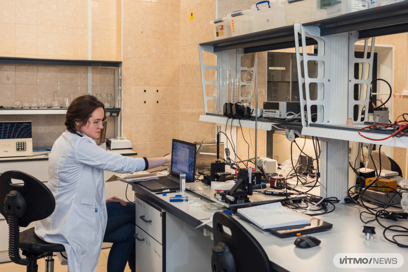
The new laboratory is meant to facilitate the development of breakthrough fields studied by the university’s researchers. One such group, for instance, is Chemotronic and Interfaces, headed by Eugene Smirnov, a participant of the ITMO Fellowship program. With an area of 300 square meters, the new lab will house more equipment and create more employment opportunities for ITMO students. There are five areas in the new facility: a storage and engineering room, an office, and separate areas for experiments in organic, inorganic, and electrochemistry.
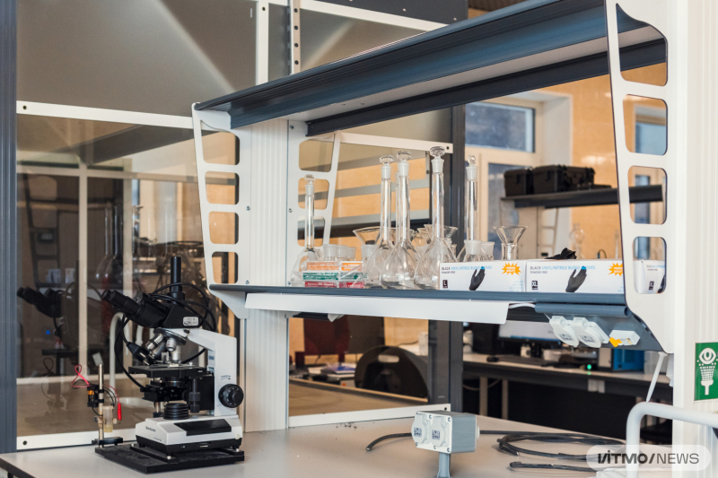
Among the available equipment are a number of specialized devices. One is a spectrometer for measuring electron paramagnetic resonance, which analyzes organic molecules and identifies unpaired electrons in molecules (such as organic radicals). Another is an infrared spectrometer meant for studying vibrations within molecules, which makes it possible to identify the compounds they contain. There are also atomic-force microscopes that can “sense” a surface on nanoscale with a special probe and visualize its microstructure in 3D. One other interesting device measures the scale and zeta-potential of colloidal solutions in order to evaluate their stability with laser scattering.
What is more, the researchers will now have a wider pool of potentiostats, which are electronic devices that manage and maintain a specified potential in a system. In the future, the scientists are planning to produce ultramicroelectrodes (UME) and modify their surfaces for a broad range of applications.
The SVET/SIET device used to measure ion and electron beams (for example, in photocatalysis and electrochemical reactions). Photo by Dmitry Grigoryev, ITMO.NEWS
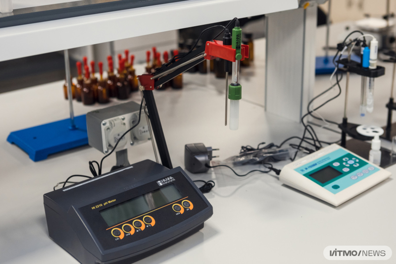
A pH meter used to measure solutions' acidity. Photo by Dmitry Grigoryev, ITMO.NEWS
Projects at the new lab
The lab will be used to conduct experiments in organic, inorganic, physical, and electrochemistry. For instance, some studies will involve the development of thin (tens of nanometers and less) films from ensembles of self-assembling nanoparticles. ITMO’s scientists have already made progress in this field: they can produce particles of any size and shape, as well as layer them onto different materials. Thanks to this, the resulting films can have different properties, which makes them applicable for use in next-gen sensors. For example, they can be used in Raman spectroscopy (a group of methods that register a substance’s scattered light) for quality and quantity analysis of low-concentration samples – on the scale of nanomoles and less, down to single molecules.
Another application for these films is optics: for instance, as a heating element in eyeglasses or mirrors that prevents condensation, which usually appears when the person wearing them enters a warm room during the cold season. If you go back outside right away, the condensed water will turn into a layer of ice, which isn’t convenient or safe – for example, during geological works in the Arctic. The films developed at ITMO will solve this problem.
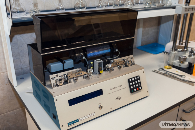
A puller for making ultrathin electrodes. Photo by Dmitry Grigoryev, ITMO.NEWS
Sensors and new materials
These days, researchers from ITMO with support from the Russian Science Foundation are developing a sensor platform that will be able to analyze various ecotoxicants (toxic chemical compounds resistant to environmental conditions), identify markers of illnesses, and detect dangerous substances depending on the surface’s modification. At the core of this method is Raman spectroscopy, which is normally used to acquire structural “fingerprints” that help identify molecules, while the intensity of their lines represents a substance’s concentration. With this method, it’s possible to conduct both quality and quantity analysis. However, the intensity of light scattering is very small and special amplifying films are needed to register it – at ITMO, these are produced from incremental gold and silver nanoparticles. The signal is amplified on an abrasive surface made from such films.
In order to make the film-based sensor even more sensitive, the film can be modified by adding to its surface some molecules that will specifically react to a certain substance or class of substances. Therefore, the resulting films will be applicable in sensors for different substances – for instance, the current project aims to detect phenol compounds in raw materials. When found in plant-based protein, these compounds can affect the taste and color of final products, which makes it important to control for their presence at each production stage.
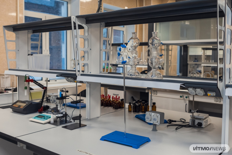
The new laboratory at the Infochemistry Scientific Center. Photo by Dmitry Grigoryev, ITMO.NEWS
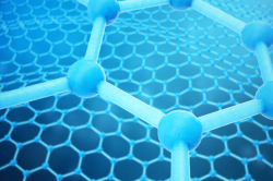
Apart from that, the lab will house an ongoing project on 2D materials, including MXenes (layered titanium carbide) and graphene-like materials. Normally, the synthesis of these materials results in particles with diameters ranging from hundreds of nanometers to tens of microns that are only 1-2 nanometers thick. Such particles demonstrate some useful physical and chemical properties. For example, MXenes’ conductivity changes depending on the degree of oxidation and the properties of surface groups. Thanks to that, this material is already used in chemotronic devices and artificial neural networks with the potential of being applied in perceptrons. Graphene and graphene-like materials, on the other hand, will be able to replace silicon in microelectronics thanks to their electroconductivity, which depends on the oxidation degree and shape of a graphene sheet – which, in turn, can be cut out with an ion beam. In order to make such applications of graphene possible, the researchers need to create films made from separate graphene scales and learn to transfer them onto different surfaces and substrates with areas of tens of square centimeters.
For this purpose, the lab’s researchers will be developing new methods of synthesizing 2D materials with the help of water transfer printing.
This year, the university is planning to collaborate with the Moscow-based Frumkin Institute of Physical Chemistry and Electrochemistry to study another 2D material, the semiconductor MoS2, which can also be used in sensors and nanoelectronics. For example, a large layer of its tightly-packed particles can be transferred to a hard silicon or glass surface; then, an electric circuit can be etched into the surface with an electron or ion beam instead of a laser. The result will be a basis for nanoelectronic devices produced without expensive lithographic masks.
Kipp's apparatuses used to produce small volumes of hydrogen. Photo by Dmitry Grigoryev, ITMO.NEWS
Food- and biotech
The new laboratory will also have facilities for research in food- and biotech. For instance, one of the promising directions is flavor modification. In collaboration with researchers from Siberian Federal University, ITMO is planning to analyze how colloid chemistry can be used to mask or enhance flavors. Moreover, scientists from ITMO are working in collaboration with Uralchem Innovation to develop pea protein-based vegan products – here, too, colloid and surface chemistry is essential.
Ekaterina Skorb, the head of the new lab and the Infochemistry Scientific Center:
“At the center, we are developing all contemporary fields at the intersection of life sciences and information technologies, including computational methods for electron structure in quantum chemistry and molecular dynamics, reaction-diffusion models, chemometrics, chemoinformatics, triboinformatics (a field that studies friction and interaction of solid surfaces using AI and big data – Ed.), AI applications in chemistry and materials science, and digitalization of various fields – from materials for regenerative medicine to food technologies, agriculture, oil production, and now chemotronics. Long-term goals for each of the fields are connected to establishing new markets, while our short-term goals are to develop basic technologies with fundamental research and use them to create products and materials in the nearest future.”
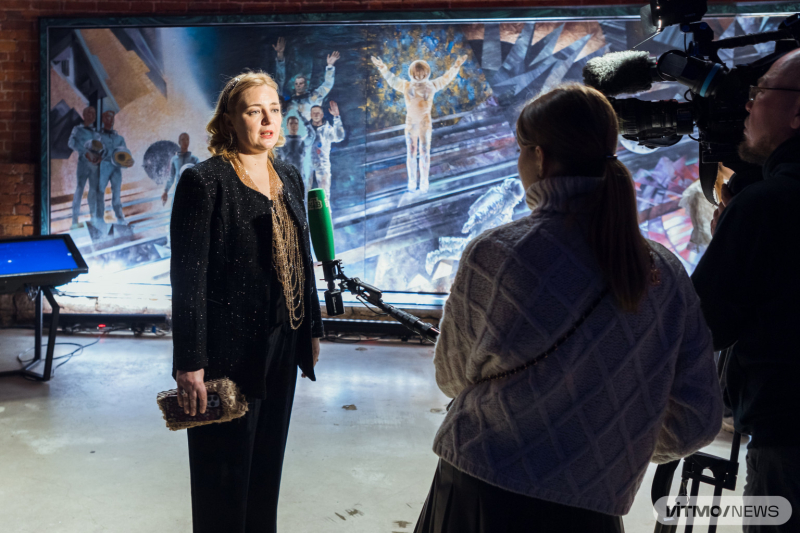
Ekaterina Skorb at the Blue Sky Research contest. Photo by Dmitry Grigoryev, ITMO.NEWS
Student-led research
At the same time, according to Ekaterina Skorb, the new laboratory was created for students – the new facility will serve as a base for studies that will turn into theses written as scientific articles. The lab will also be open to school students, who will conduct their projects there within the national initiative Sirius.Summer.
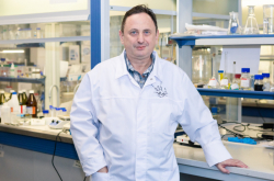
Eugene Smirnov, a professor at the center and a leading researcher:
“We are planning to also introduce Friday Fun – to free up some time on Fridays or Saturdays so students would be able to conduct their own experiments. In my own day, I remember making strawberry and raspberry juice to compare their colors with a spectrometer. It’s not just fun, it can also pave the way to a discovery. For example, the physicist Andre Geim and Michael Berry received the Ig Noble Prize for their experiment with a levitating frog with a superconductor in a magnetic field, which sounds fairly bizarre. Later, Andre Geim and Konstantin Novoselov received an actual Nobel Prize for their work on graphene, having peeled off a graphene layer from a pencil. I hope that our students will be just as curious in bringing their ideas to life.”
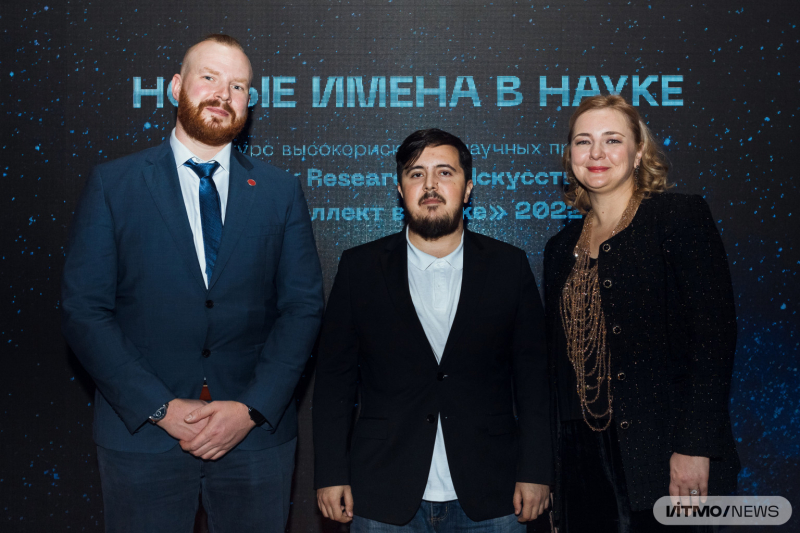
Eugene Smirnov, Timur Aliev, and Ekaterina Skorb at the Blue Sky Research contest. Photo by Dmitry Grigoryev, ITMO.NEWS