The research
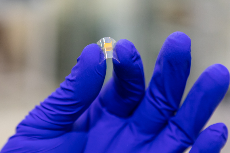
The staff of ITMO University’s Laboratory of Hybrid Nanophotonics and Optoelectronics (PeroLab) have recently unveiled a unique geometrical structure that consists of a film layer of carbon nanotubes (electrodes), polyethylenephthalate (flexible polymer substrate), and perovskite microcrystals (photosensitive element). The resulting product can be used in flexible electronics.
The researchers have demonstrated that their prototype is capable of retaining its functional properties in its regular state as well as when bent. In particular, its initial properties did not experience any significant change even after mechanical stress testing, which entailed 10,000 cycles of elastic deformation.
Usually, perovskite-based optoelectronics use metal electrodes, such as those made of gold or silver. But regular interaction with perovskite ions results in their gradual deterioration. For that reason, the scientists used electrodes made of a film consisting of 20 nm carbon nanotubes.
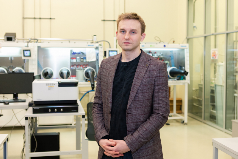
Alexandr Marunchenko, a PhD student at ITMO’s Faculty of Physics, became the article’s lead author.
“I got my Master’s at Skoltech, where I worked at Albert Nasibulin’s (a co-author of the article – Ed.) Laboratory of Nanomaterials. They are, perhaps, the top experts in Russia on the synthesis of single-walled carbon nanotubes. When I came to ITMO for my PhD, I began to study another material: crystals of halide perovskites. I was able to combine knowledge of these two subjects by utilizing their properties in one device,” he explains.

Alexandr Marunchenko. Photo by Dmitry Grigoryev, ITMO.NEWS
The assembly
The proposed device’s operating component are perovskite crystals installed between two carbon nanotube electrodes. If these electrodes are placed far apart, the charge generated by the photodetector may disperse while trying to reach them and thus the signal will not be detected. The researchers’ goal is to avoid this happening.
To that end, they slice a film made of carbon nanotubes into two “ribbons” with a precision down to a single micron. This is done using a femtosecond laser; this method provides enough energy to the photon pulse to cut the electrode material while also keeping the polymer substrate intact. The gap between the two electrode ribbons is filled in with a conductive material – a perovskite. The crystals are synthesized right on the spot at low temperature.
“We optimized the synthesis of perovskites in such a way that the sensitive element of our photodetector would contain as many crystals as possible. This allows us to produce a strong photoinduced signal,” explains Alexandr Marunchenko.
Flexible electronics are a class of electronic devices with one notable trait: they all can be twisted and bent without any negative effects on their functional properties. These properties are instead affected by the qualities of the materials used in the operating component as well as the substrate on which the device is assembled. The researchers used polyethylenephthalate for the substrate; however, such devices could be constructed on other flexible substrates, too.

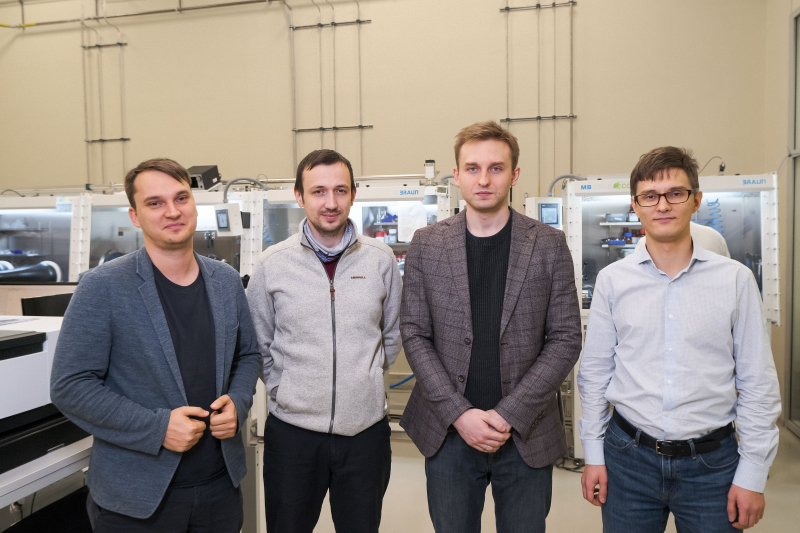
The team of the project (left to right): Sergey Makarov, Dmitry Gets, Alexandr Marunchenko, and Anatoly Pushkarev. Photo courtesy of ITMO's Faculty of Physics
How it works
In the dark state, the current within the photodetector is defined by the material; when subjected to light, it is defined by the charge carriers generated within the perovskite. As they impact the sensitive element, photons are converted into electron-holes that are collected by the carbon nanotube electrodes.
“The geometry we’ve proposed is quite simple, cheap, and effective. It could be used to work with other materials, not just perovskites. What’s important is that this simple prototype will help us in the future to create and improve more complex and multi-functional optoelectronic devices,” says Alexandr Marunchenko.
The advantages
What makes this project unique is that it marks the first time that researchers have used a carbon nanotube film to create electrodes for a perovskite-based photodetector. This solves the main challenge faced by such devices – the issue of their longevity. In addition, the prototype’s simple geometry, inexpensive material, and low-temperature synthesis of the perovskite ensure the low cost of its assembly.
According to the scientists, the resulting photodetector has been found to be 1,000 times more efficient than its commercially available silicon-based counterparts. The reason for this is the close proximity of the electrodes inside the device.
In the process, the researchers also optimized a number of processes and understood how to combine two materials that had not been used together before. The geometry used in the device is quite versatile and may be used in many other electronics. With this device, the team has demonstrated that the proposed approach can boast a number of qualities suitable for other practical applications.
“The demand for flexible electronics is rising in light of the interest in wearable devices. They’ll be integrated into clothes, among other things, and be lightweight, compact, low-consumption, and autonomous, as well as capable of transmitting data to your phone. It’s highly useful for health monitoring, so you could have a device collect information in real time about your pulse and the levels of oxygen, sugar, and other substances in your blood. A key parameter for such devices is not only their flexibility, but also the sensitivity that can be achieved using various cutting-edge materials and architectures. Our device corresponds to these needs, and now we’re ready to begin upscaling the prototype and testing it in conditions close to those of real-life use,” notes Sergey Makarov, the head of ITMO University’s Laboratory of Hybrid Nanophotonics and Optoelectronics.
Reference: Alexandr A. Marunchenko, Mikhail A. Baranov, Elena V. Ushakova, Daniil R. Ryabov, Anatoly P. Pushkarev, Dmitry S. Gets, Albert G. Nasibulin, Sergey V. Makarov, Single-Walled Carbon Nanotube Thin Film for Flexible and Highly Responsive Perovskite Photodetector (Advanced Functional Materials, 2021).


