ADOPSYS project was launched in 2013 with the support of the Marie Skłodowska-Curie Actions grant system as part of the European Union’s 7th Framework Programme. Seven European universities, including ITMO University, as well as a number of commercial businesses, formed an educational consortium to train highly-qualified specialists in the field of optical systems design. ADOPSYS has two main goals: to create new optical methods and components in close collaboration between scientific and academic institutions and the industry, as well as to develop a unique European infrastructure for the training of young photonics and optics scientists.

12 young researchers participated in the project, each training at one of the participating universities while exchanging experience with researchers at the various partner universities, among which were: the Free University of Brussels (Belgium), Institut d'optique (France), Technical University of Madrid (Spain), University of Jena (Germany), University of Eastern Finland and ITMO University. Students also paid regular visits to the leading European companies working with IT, optics and interdisciplinary quality-of-life research: Carl Zeiss, Datalogic, Osram, ASML, TNO and Phillips.

ADOPSYS, therefore, has a very strong practice-oriented nature. In the official press release marking the end of the ADOPSYS project, its coordinator Paul Urbach, who is a professor at the Delft University of Technology (the Netherlands) and a member of ITMO’s International Council, had this to say:
“Often the focus in universities is on newer topics such as nano-optics or meta-materials whilst optics, of more relevance to industry, is less addressed. This is especially true for optical design of lens and mirror systems for imaging and non-imaging applications”.
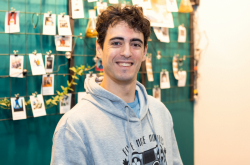
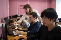
As part of the project, ITMO University hosted Nenad Zoric, a young engineer from Serbia (we’ve previously written about Nenad here), who was provided an individualized curriculum plan and conducted his research at the Research Laboratory for Computer-Aided Design of Optical-Information and Energy Saving Systems under the supervision of Irina Livshits, head of the lab. Over the course of three years, he learned the computational methods for complex photolithographic optical systems and wrote a thesis work based on his studies.

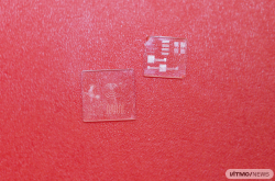
Photolithography is used it microelectronics. It can be used to create images on silicon plates to produce specific properties in the operation of microcircuits. Images are made with photoresists – light-sensitive materials subjected to specific wavelengths through masks. To make microcircuits smaller, which is the current trend in microelectronics, the images, too, must become smaller. In order for that to happen, optical systems and the precision of photolithographic tech must be improved.
Today, only a few companies in the world produce these complex mechanisms, among them ASML (the Netherlands) and Carl Zeiss (Germany). Even then, only a few dozen copies are made a year, as they are highly complex and include a large number of components. This means that highly-qualified specialists are very much in demand in this field.

“Computational methods used for such systems tend to be company know-hows. Modern technology is developing very quickly and we’re in a situation where one new technology requires us to upgrade the others, resulting in a closed loop of constantly increasing complexity of optical systems. For instance, the resolution power of matrices is constantly growing, meaning that we need new lenses or, inversely, a new lens can’t be used with obsolete receptors, etc. This is why research and production today should occur simultaneously instead of following each other,” – explains Roman Anitropov, lead programmer at the laboratory.
He adds that the laboratory is always working together with major optical systems makers from all over the world in order to carry out research in the areas that are most beneficial to the industry. Besides, contact with industrial partners lets them find more effective solutions for optical systems design, the knowledge of which is then passed on to the students.

Now that the ADOPSYS has ended, the lab plans to continue taking part in the European Union’s framework projects, including the Horizon 2020 initiative. The lab has already won a grant to train European students as part of the Erasmus program. Its staff is also working on a collaboration with Chinese partners, as China has one of the largest production capacities for optical systems.
“Our lab is interested in attracting new talent, including students, who will be able to receive education that adheres to the European standards of quality and receive invaluable experience; in the future, the best students will be able to apply for work here,” – says Roman Anitropov.


