Crystals are solids with a periodic structure, i.e. when atoms are displaced, they take the exact places of other atoms, in which the latter were before the shift. This fact was scientifically proved at the beginning of the 20th century. It gave rise to modern solid-state physics and also laid the foundation for the development of semiconductor technologies.
“Computers, smartphones, LED bulbs, lasers – everything we can’t imagine our day-to-day lives without,” says Mikhail Rybin, Associate Professor at ITMO’s Faculty of Physics and Engineering, “was designed thanks to the fact that we understand the nature of the crystalline structure of semiconductor materials. The theory of periodic structures allows us to conclude that waves – be it light, electrons, or sound – can only move in two ways. Either the wave propagates forward in the crystal, or it rapidly fades at the frequencies of the so-called band gap. There are no other options and it greatly simplifies the laws of particle propagation while facilitating engineering tasks”.
However, some devices require the crystal to not transmit the wave and not extinguish it either, but to retain it in itself for some time – something like a light “trap” is needed.
“For example, for laser or sensors operation, the wave must pass through the working area of the device several times to enhance the efficiency of its interaction with an active element,” explains Mikhail Rybin. “It's especially crucial to create such a "trap" for light because it is very difficult to keep it in a small area. It is an important technological challenge for modern physics”.
The bigger, the better
Ideally, the entire material should take on the role of a “trap”, because the more light is captured, the more efficient the interaction of the wave with the active substance will be. However, in the case of a crystal, it is not possible. As stated earlier, it can only extinguish the wave or let it pass through.
“Alternatively, there is a possibility of localizing light in disordered structures, for example, in powders,” notes Mikhail Rybin. “However, we cannot achieve reproducibility in such systems. In one sample, the particles were arranged in one way, and in another – completely differently. For applied tasks, you need something suitable for mass production of the same devices”.
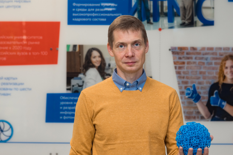
There is also a third way. We can use an intermediate type of materials in which the particles do not form periodic lattices, as it happens in crystals, but at the same time have a mathematically strict ordering. These structures are called quasicrystals, they were discovered in the 1980s and have been studied by physicists ever since.
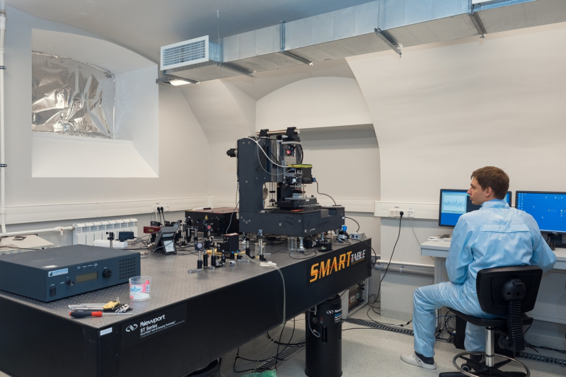
“Since there is no periodicity in quasicrystals,” says Mikhail Rybin, “there is also no restriction that the wave can either pass directly without loss or disappear quickly. A paper published in 2017 predicted the phenomenon of light localization in quasicrystalline structures, and we had to confirm it experimentally.”
Easier said than done
During almost 40 years of studying quasicrystals, physicists have understood their structure and learned to model it on a computer. The problem is that such quasicrystals are not so easy to synthesize on the microlevel.
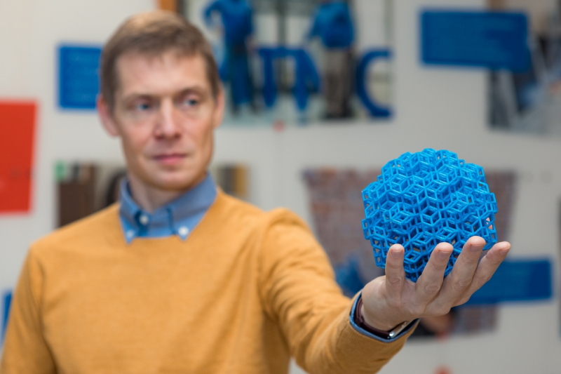
“That’s when the development of technology comes to our rescue,” says Artem Sinelnik, a PhD student at the Department of Physics and Engineering. “At our faculty, there is a setup for three-dimensional nano-printing, where a voxel (the minimum volume of printing – Ed. ITMO.NEWS) is about half a micron, which is a hundred times smaller than a human hair. With its help, we created the structure of a quasicrystal with a complex structured distribution of the material in three-dimensional space.”
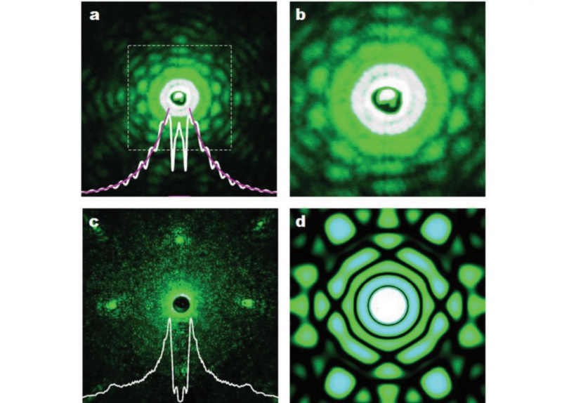
After creating the samples, the scientists started their preliminary study. They analyzed the surface quality with an electron microscope. Then, they proceeded to optical measurements to confirm that the internal capacity of the sample really does have a quasicrystalline structure.
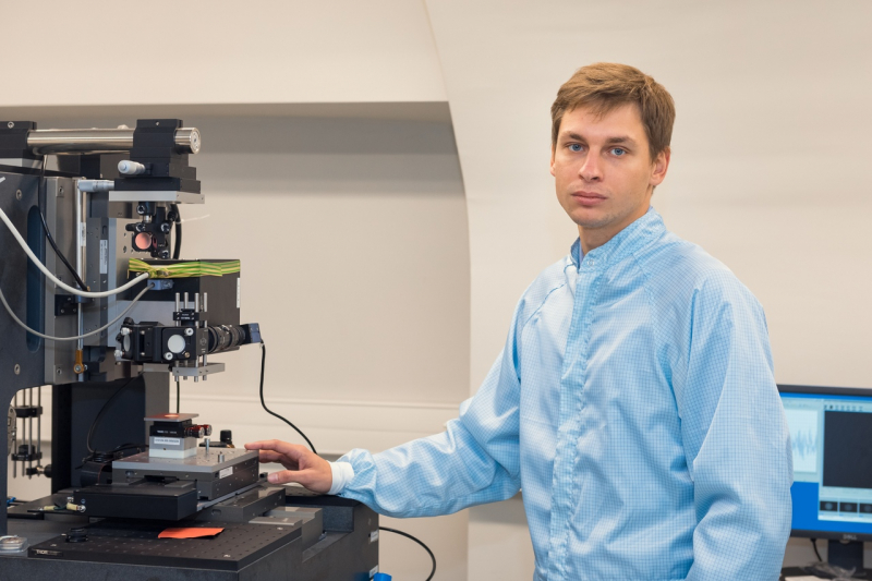
“After that, we did an experiment,” explains the co-author of the work, Artem Sinelnik, “a short light pulse was sent to the quasicrystal and the so-called afterglow was measured. As it turned out, light exits our samples with a delay, that is, the wave is held inside for quite a long time. Thus, we have confirmed the ability to capture light in a three-dimensional polymer quasicrystal.”
Prospects
For now, the work is solely fundamental. It demonstrates the main optical properties of polymer quasicrystals, created by using three-dimensional nano-printing, and their ability to localize light. However, as the authors note, the study may be applied in the future.
“For example, usually a laser is designed based on the fact that we have an active medium in which light gets localized via a sufficiently large external resonator,” explains Mikhail Rybin. “In this work, we have shown that a quasicrystal can combine the functions of an active medium and a resonator in a single structure.”
Reference: Artem D. Sinelnik Ivan I. Shishkin Xiaochang Yu Kirill B. Samusev Pavel A. Belov Mikhail F. Limonov Pavel Ginzburg Mikhail V. Rybin. Experimental Observation of Intrinsic Light Localization in Photonic Icosahedral Quasicrystals. Adv. Optical Mater. 2020/10.1002/adom.202001170
