About one-atom-thick, monolayer semiconductors are a relatively new class of metamaterials that have been actively studied over the past decade. They hold a great potential for optical information processing technologies – computers, controllers, communications, and so on. Their main advantage is ultraefficiency and low energy consumption, ensured by the fact that light travels faster and more efficiently than charged particles in solids.
While replacing electronic chips with optical ones will constitute a significant technological breakthrough, there are still physical limitations to overcome. In order for optical elements, including switches, to be integrated with each other on a microchip, they have to be smaller than the wavelength in the visible spectrum (which is measured at 380-760 nanometers). In other words, they have to be less than 100 nanometers in size; the smaller – the better.
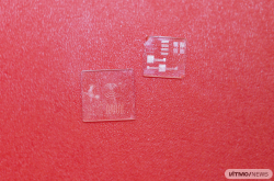
Researchers from ITMO’s School of Physics and Engineering have managed to produce just such a structure – their optical switch is under 10 nanometers in every dimension, making it 100 times smaller than the wavelength of light.
How it works
At the core of the new device is plasmon resonance. Two monolayer semiconductors (each 3 atoms thick) are placed inside a nanoresonator made of gold particles (5-10 nanometers in size). Each layer contains excitons – quasiparticles carrying excitation without transferring their charge – that are distributed in a certain way. If this structure is subjected to light with a specific phase front, then the excitons shift towards the edges or the center of the plasmonic nanoresonator. The switch of excitons between these two conditions corresponds to 1 and 0.
According to the researchers, these ultracompact switches haven’t been studied before:
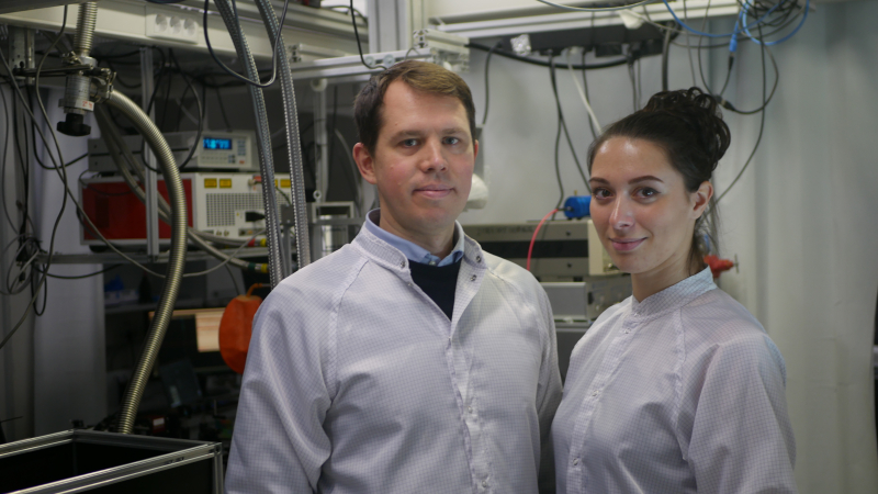
“The idea of switching between different exciton states is rather novel. Moreover, we are the first to have used 2D semiconductor heterostructures combined with a plasmon resonator. This innovation allowed us to make the switch 100 times smaller,” explains Vasily Kravtsov, an author of the paper and a lead researcher at the School of Physics and Engineering.
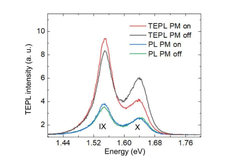
A demonstration of switching without the gold particle, maintaining the polarization. Illustration from the article
What’s next
The new device is easy to manufacture: according to Dr. Kravtsov, even school students can remove monolayers from a crystal. Scaling, however, is an issue: the proposed method can produce monolayers only up to several hundred microns in size. The world’s leading tech giants are working on an approach that can produce larger monolayers of high quality, but so far without success.
The university’s researchers will be focusing on improving the switch’s properties rather than scaling. First, its precision is now under 90% – and this can be solved by adjusting the geometry and design of the resonator.
Second, the scientists want to create a system with three layers instead of two: this would mean that the switch has more than two exciton states. Third, the switching can become ultrafast – for instance, if the structure is subjected to a femtosecond laser.
This study is supported by the federal program Priority 2030 and two Russian Science Foundation grants (21-72-10100 and 22-72-10047).
Reference: Yeonjeong Koo, Hyeongwoo Lee, Tatiana Ivanova, Roman S. Savelev, Mihail I. Petrov, Vasily Kravtsov, Kyoung-Duck Park. Nanocavity-Integrated van der Waals Heterobilayers for Nano-excitonic Transistor (ACS Nano, 2023).